
ReRAM: The Next-Gen Memory

Resistive Random Access Memory (ReRAM) is one of the primary contenders to become the next generation memory technology in the near future. Among several other reasons, the most important reason is the non-volatile nature of ReRAM. Every non-volatile memory is getting massive attention from researchers and manufacturers currently. That makes it a race between different technologies targeting the standard level of performance goals with almost the same advantages.
Each non-volatile memory is fighting neck to neck to establish itself as a reliable contender of memory. MRAM (Magnetoresistive), FeRAM (Ferroelectric), and PCRAM (Phase Change) are other non-volatile memories of today's interest. So, what makes ReRAM unique and able to compete with these technologies? The high read and write speed make it different from others. Also, the fabrication of ReRAM is not that complex compared to others.
On the other hand, the factors limiting its establishment in the market are low reliability and performance variations. So, it still needs massive development in fabricating material, structure, circuit issues, and dealing with undesired disturbances from the external environment. The above advantages appear to outweigh the limitations and make ReRAM technology very promising for the future.
Device Architecture of ReRAM
ReRAM is a Metal-insulator-Metal structure wherein the insulator is sandwiched between two metal layers. If touched, both the metals form a low resistive state, and if they do not touch, they form a high resistive state. The central functioning part of the structure is a conducting filament. Depending upon the applied voltage across the metal terminals, a formation or rupture of the filament occurs.
This structure can be interpreted as a bridge between two mountains separated due to a ditch. However, the bridge is not connected to the mountains unless a necessary push(voltage) is provided to the bridge. When there is the proper voltage across the ends of the bridge, the bridge lowers and meets another mountain, making a path easy to cross. So, when a voltage is applied differently, it breaks the bridge, and the bridge loses touch with another mountain, making it challenging to cross.
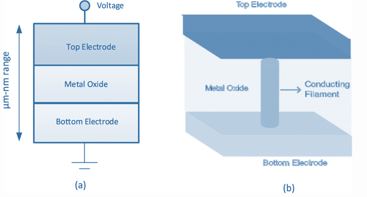
(a) 2D structure of ReRam (b) 3D structure of ReRam (Source : Lumenci)
How Does a ReRAM Work?
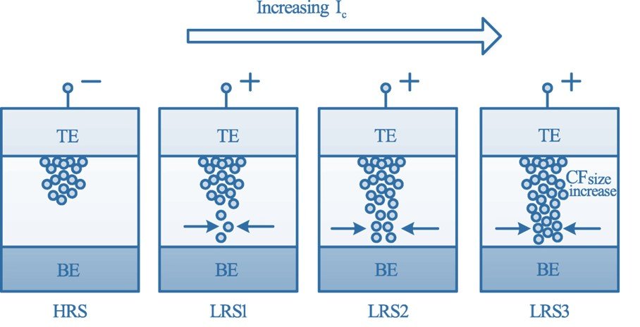
ReRAM can store digital data (or 0's and 1's), which is attributed to the structure of ReRAM. ReRAM is one of the primary contenders to become the next generation memory technology in the near future. Among several other reasons, the most important reason is the non-volatile nature of ReRAM has multiple resistive states mapped to digital logic. Usually, ReRAM has a High Resistive State [HRS], i.e., logic low referred to as 0; a voltage is applied across ReRAM to switch its state from the High Resistive State to a Low Resistive State [LRS], i.e., logic high referred to as 1. Since the filament is in a detached state during the HRS, there is no proper path for the current to flow

High resistive state (HRS) (Source : Lumenci)
When a suitable voltage is applied across the top electrode (TE) and bottom electrode (BE), the filament meets the bottom terminal and forms a low resistive path, i.e., comes into LRS; in other words, logic high, which is referred to as 1. HRS is the OFF state, and LRS is the ON state.

Low resistive state (LRS) (Source : Lumenci)
The voltage applied to change ReRAM state from HRS to LRS is the 'Set' voltage. Similarly, the voltage applied to change the state from LRS to HRS is the 'Reset' voltage.
The formation or rupture of the filament occurs after a voltage is applied, which is more than the Reset or Set voltage. This state change is the write operation while putting ReRAM in the desired state to hold a logic. To read the operation, a small voltage is applied, which is less than the Reset or Set voltage, and the output is sensed to know the state of ReRAM. This resistive switching can be of two types depending upon the polarity of applied voltage. It can be either unipolar or bipolar. In unipolar switching, the switching is independent of the polarity of the voltage. In contrast, in bipolar switching, the switching depends on the polarity of voltage, i.e., HRS to LRS in one polarity and LRS to HRS in the other polarity.
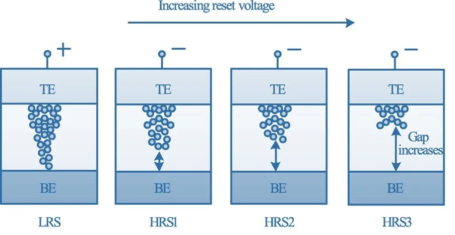
Formation and Rupture of Filament depending upon the applied voltage of a different polarity (Source: Lumenci)
Types of ReRAM
1. CB ReRAM
The Conductive Bridge ReRAM (CB ReRAM) is a metal-dielectric metal structure. The formation of a bridge between the metal electrodes occurs due to the breakdown of dielectric and ionic transport. The process is reversible; it is possible to switch the resistive state. As explained above, the device architecture, logic states, and working principles are like ReRAM.
2. Ox ReRam
Metal-Oxide ReRAM has a metal oxide metal structure. The switching and filament formation occurs due to oxide breakdown depending on the applied voltage. The arrangement of oxygen valences generated due to the breakdown of oxide leads to the formation of the bridge(filament).
As explained above, the device architecture, logic states, and working principle are much like in ReRAM.
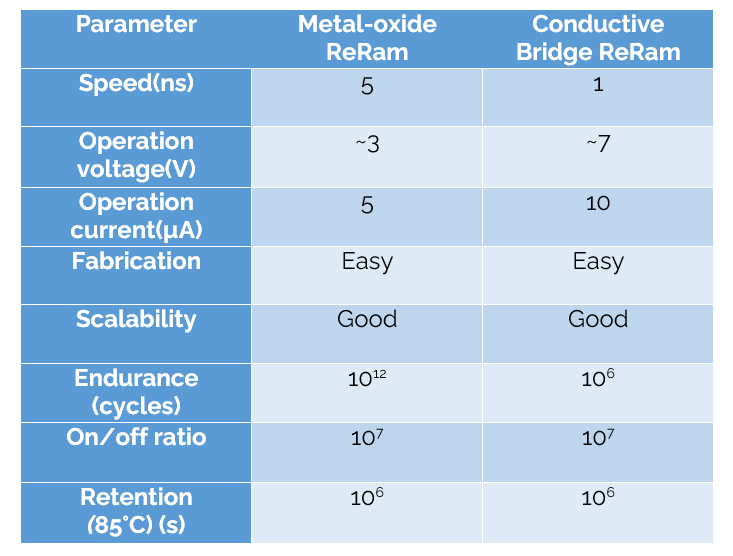
Comparison of CB ReRAM vs Ox ReRAM
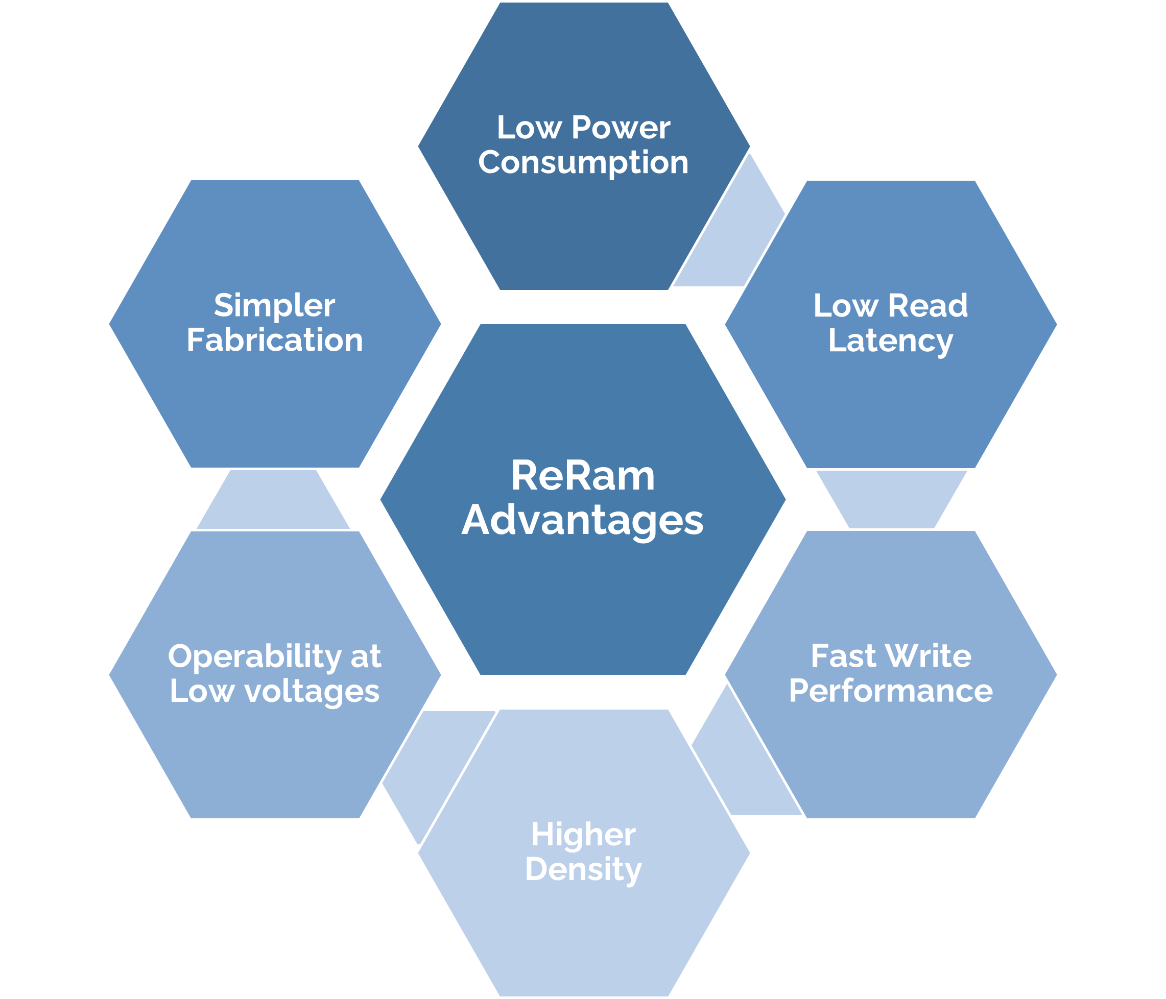
ReRAM Advantages
How does ReRAM compare with other NVMs?
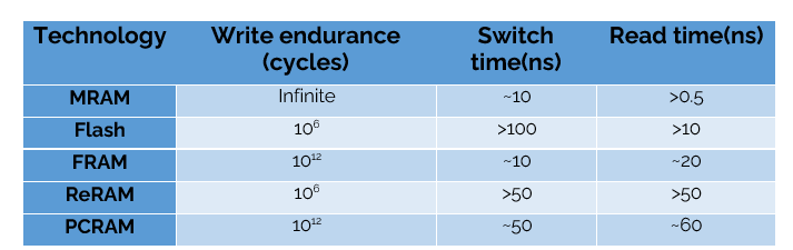
The above table shows a performance comparison of ReRAM with other technologies. ReRAM shows less endurance than MRAM, FRAM, and PCRAM but offers a higher switch time than Flash and a comparable switch time against PCRAM. Also, ReRAM has a better-read time than PCRAM. MRAM comes out to be the best when endurance cycle, read time, and write time are considered for comparison. The above comparison shows that ReRAM comes behind FRAM and MRAM in performance. However, ReRAM manufacturing is much simpler than these two memories, putting ReRAM ahead in the race.
What does the Patent Landscape look like?
The number of patents filed related to ReRAM technology appears to be increasing over the years, as shown in Fig:2 (below). A significant increase in the filed patent can be seen after 2010, as shown in Fig:2. It indicates that the major tech companies, researchers, and academic institutions are interested in ReRAM.
Fig:1 (below) shows that the major tech companies hold a substantial number of patents related to ReRAM, which indicates a stronger growth rate for ReRAM. ReRAM can replace the existing semiconductor memory technologies such as DRAM with further advancements.

Fig:1 - Count of patent families (Source : Lumenci)

Fig.2 : Yearly trends of patent families (Source : Lumenci)
As per Fig: 3, the US has filed the most patents for filing countries, followed by China, Korea, and Japan. The data shows that the most significant number of patents filed or granted was in 2019, followed by 2018, 2017, and 2020. There is a decrease in number in the year 2020 and 2021 relative to previous years; this might be because the entire world faced a significant pandemic. It might also be possible that ReRAM technology has matured to an extent where further development in technology is only possible when other related fields such as new materials, fabrication processes, supporting technologies, etc., will grow.

Geographical distribution of patents for Wi-Fi 6 technology
**We have included alive PCT applications (last 31 months till March 2022) - WO
(Source : Lumenci)
The companies investing in ReRAM technology are big players in the semiconductor memory industry. As the data shows, Samsung Technology has the most significant number of patents related to
ReRAM followed by Micron and SK Hynix. Other major companies also hold a sizeable number of patents. Having more patents does not imply that this company is putting the most effort but shows that these companies are showing a lot of interest in this technology and will keep putting efforts to make it even better.
Lumenci's analysis shows that many patents are usually related to the manufacturing of ReRAMand solving issues related to its structure or behavior that reduces the performance. Overall, the patent landscape analysis shows that ReRAM is still growing, and in the future, it will have a significant impact on the memory technology market.
Pros and Cons
Firstly, let us begin with the pros. ReRAM consumes less power than NAND and has higher read and write speed; it is highly scalable up to a few nanometres and has high retention and storage density. The non-volatile nature may be the rudimentary but most significant advantage of ReRAM. On the other hand, ReRAM is still in the developing phase. The switching speed is not on par with Flash memory. The repetition cycle is also limited to traditional values. One of the biggest cons of ReRAM is its performance variation due to temperature effects.
One of the most significant limitations for ReRAM is its compatibility with CMOS technology. The sneak path limits the performance of ReRAM. Sneak paths are unexpected paths in the RAM circuit along which current, energy, or logical sequence flows in an unintended direction. Also, the ongoing scalability is another significant limitation for ReRAM. A minimal filament formation might not hold the characteristic of a standard ReRAM filament and might lead to a change in the working and performance. The limited repetition cycle is also an issue.
The regular advancement might lead to an increase in the number of repetition cycles. The future ReRAM will have even better switching speed and retention. Also, with proper advancement, the scalability issue with the filament may be resolved and lead to even better performance. It will not be a memory alone, but in the future, with proper advancement, it may become a computing unit for neuromorphic networks, AI, and ML-related applications. ReRAM is still growing, and with appropriate improvement and more growth, ReRAM can be the future technology that can change the world. Also, ReRAM is highly appreciated in the IoT domain and its wide range of applications in domains such as mobile phones, robotics, tablets, automobile electronics, etc.
*Disclaimer: This report is based on information that is publicly available and is considered to be reliable. However, Lumenci cannot be held responsible for the accuracy or reliability of this data.
*Disclaimer: This report is based on information that is publicly available and is considered to be reliable. However, Lumenci cannot be held responsible for the accuracy or reliability of this data.
Author

Rohan Kumar
Associate Consultant at Lumenci
Rohan has experience in the IP domain and worked on multiple service lines, including Patent monetization, Portfolio Analysis, Infringement Analysis, OTT, Technical Analysis, EoU/Claim Charts, Sensors, Electronics, semiconductor fields, etc. Rohan is a Master of Technology in Sensor and IoT from the IIT Jodhpur, India.