
High Bandwidth Memory (HBM3)

High Bandwidth Memory (HBM3)
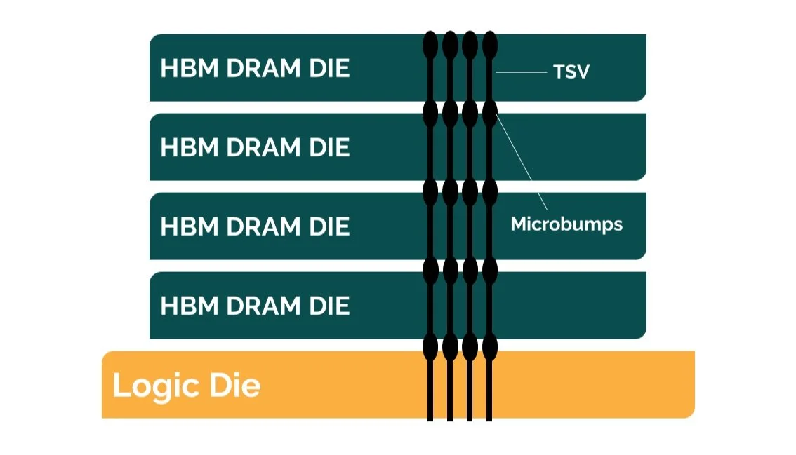
Technology domains such as AI applications, high-end servers, and graphics require fast processing and high densities for storing the data, where High Bandwidth Memory (HBM) provides the most viable memory technology solution. HBM is a three-dimensional DRAM technology with stacks of multiple DRAM dies, which are interconnected by TSV (Through-Silicon Vias), and microbumps. It is tightly coupled to the host compute die with a distributed interface. The interface is divided into entirely independent interfaces called channels and not necessarily synchronous to each other. The HBM DRAM uses a wide-interface architecture to achieve high-speed, low-power operation.
Like any other DRAM, HBM memory is controlled by commands from the host memory controller. It provides two independent row and column command interfaces, allowing activates/precharges to be issued in parallel with read/writes, and therefore this simplifies controller operations and increases efficiency. It processes 128 bits of data at a time and supports 2n prefetch architecture with 256 bits per memory read and write accesses.
High-bandwidth Memory key Features
Independent Channels
HBM DRAM is used in Graphics, High-Performance Computing, Server, Networking, and Client applications where high bandwidth is a key factor. HBM organization is similar to the basic organization of all current DRAM architectures with an additional hierarchical layer on top of it. HBM3 comprises a stack of multiple DRAM devices across several independent interfaces called channels. As per JEDEC, in HBM3, each DRAM stack can support up to 16 channels compared to 8 channels in HBM. And it is up to the vendor how these channels are distributed among the DRAM dies within the stack, but access within the channel needs to have the same latency for all accesses.
Since each channel is independent, they are discretely clocked and provide access to a distinct set of DRAM banks via independent command and data interface such as Data, Column, row address, DBI, Strobe, Clock, etc.
Pseudo Channel Mode
HBM3 has a pseudo channel mode architecture which was introduced in HBM2 standards, which divides a channel into two individual sub-channels of 32-bit I/O each as compared to 64-bit I/O in HBM2. On each segment, a read or write transaction transfers 256 bits in a burst that consists of 8 cycles of 32 bits each. Both pseudo channels operate semi-independent, i.e., channels share the same address and command bus but decode and execute commands individually. One can send a command and address to one pseudo channel or the other, but not to both.
Both Pseudo channels also share the channel’s mode register. All I/O signals of DWORD0 and DWORD1 are associated with Pseudo channel 0 and Pseudo channel 1, respectively.
Dual-Channel Interface
HBM3 DRAMs have a wide I/O interface; HBM deploys separate column and row address pins. These interfaces increase command bandwidth and performance by allowing column-related commands, i.e., read and write, to be issued simultaneously with other row-related commands, i.e., activates and precharges.
Bank Group
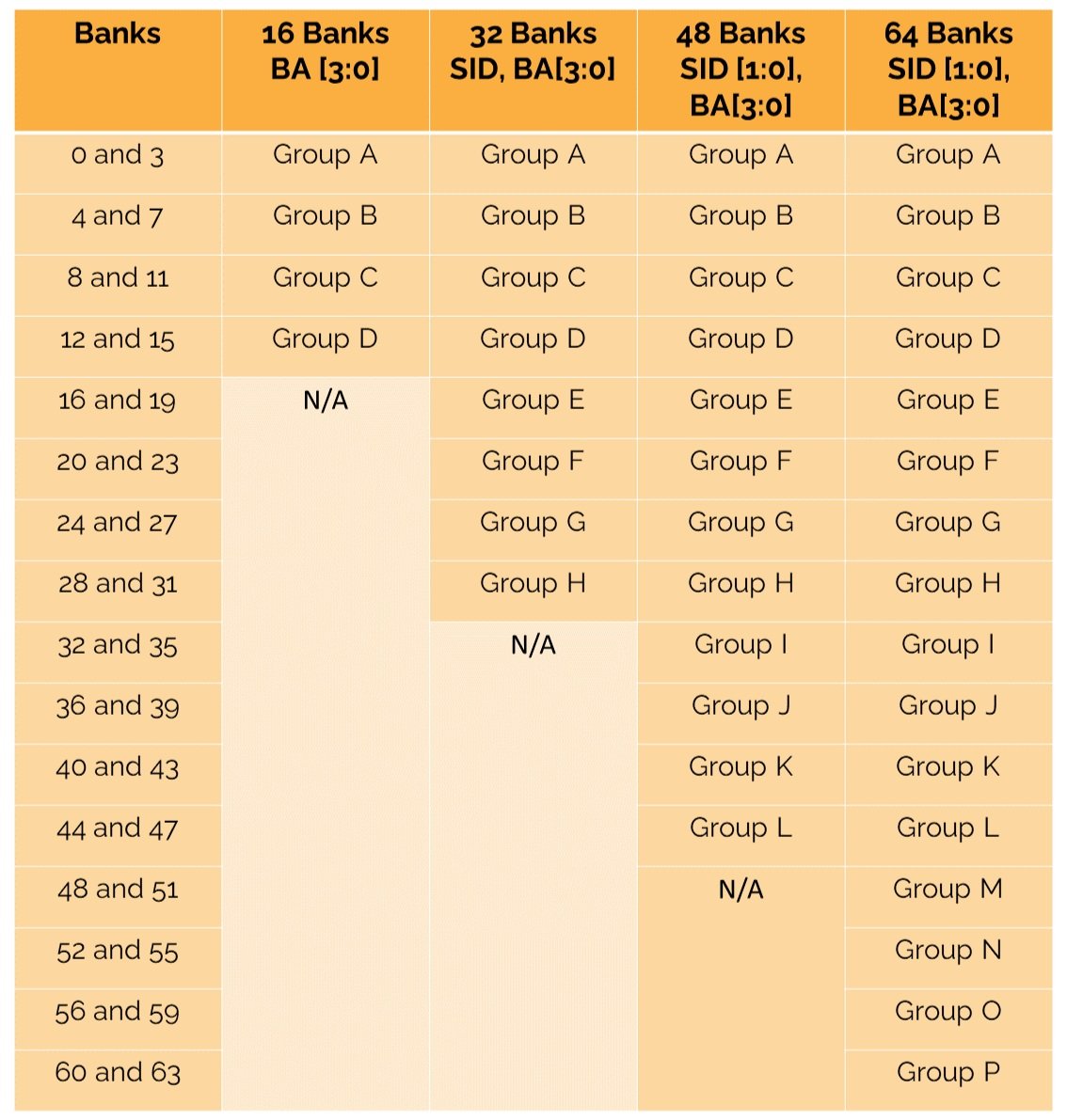
The HBM memory channel is divided into multiple banks, each bank has multiple rows, and each row has multiple columns. The banks within a device are divided into 4 or 8 or 12, or 16 bank groups. The assignment of banks to bank groups is shown in Table 5. The activity within a bank group must be restricted to ensure the proper operation of the device for HBM.
Power Up phase and Initialization Phase
The HBM operation begins with the power-up phase. The power-up phase involves issuing a reset. The channel is stuck in the power-up phase until this reset is issued. RESET signal must be maintained LOW with stable power. The channel moves on to the initialization phase once it detects the reset.
This phase is entered as soon as a reset is detected. After some time interval, RESET is de-asserted, Clock must remain LOW, and the HBM device RESETS into a precharged power-down state. After that, the HBM3 device will read and apply internal fuse configuration data and perform I/O driver impedance calibration. In addition, the model implements checks for the initialization sequence.
After driving various output signals to valid levels as per the initialization protocol issue, MRS commands to configure the HBM3 device appropriately for the application setting.
Mode Registers
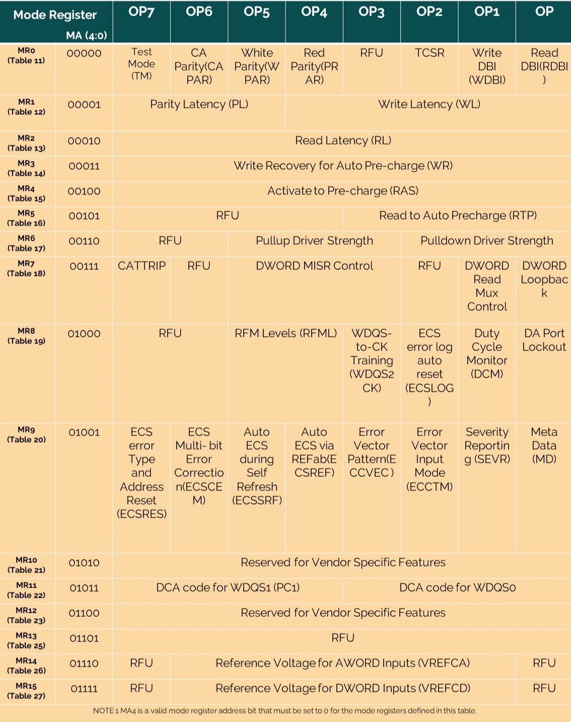
The Mode Registers are used to configure the different functionality of the HBM3 DRAM. Each HBM channel contains 16 mode registers of 8-bit each. These registers specify the mode of operation and are programmed via MRS commands before the memory is accessed. Out of these, MR10 and MR12 are special mode registers reserved for vendor-specific features.
Other key differentiating features in HBM3
First, HBM3 utilizes two types of clocks, i.e., DDR clock for command and DDR WDQS clock for data. The WDQS clock, which is twice the command clock's frequency, is driven by the controller for both read and write operations. The controller comprises a reset-type clock divider in the WDQS clock tree to generate a dual clocking frequency.
In addition, Similar to training in DDR5 and LPDDR5 memory, HBM3 has also introduced new training, i.e., WDQS-to-CK alignment (Write Leveling), WDQS Oscillator, and Duty Cycle Correction. WDQS-to-CK alignment training allows the host to observe the phase offset between the WDQS strobes in pseudo channels and the clock. WDQS Oscillator training adjusts the WDQS clock tree delay varied due to HBM3’s voltage and temperature change.
HBM3 also has a provision for symbol-based on-chip ECC calculation where symbol size is implementation-specific. HBM3 on-chip ECC has two severity pins per PC to indicate the error severity. HBM3 devices use read/write meta-data bits, error scrubbing mechanism, error transparency protocol, and fault isolation limits, which will help achieve high system Reliability, Availability, and Serviceability (RAS).
HBM v. GDDR5
Over the past decade, GDDR5 has been an industry standard and has reserved a prominent place in all graphics-oriented technologies. GDDR5 is focused on using more power to achieve greater clock speeds. GDDR5 chips are attached directly to the graphics card in a single layer, which means adding more memory involves spreading out horizontally on the graphics card. Power consumption and form factors have thus been major concerns. HBM3 provides one of the best form factors with a 16-channel stacked architecture. HBM has emerged as an alternative that breaks all processing bottlenecks.

HBM vs GDDRS : Per package comparison (Source: Lumenci)
As shown above, HBM memory offers higher bandwidth than GDDR memory and allows more memory in less space, but the cost for one HBM chip is higher than GDDR memory. HBM outruns GDDR in terms of performance, but because of the cost factor of commercial graphic cards, manufacturers prefer GDDR, although performance suffers. For the professional segment or applications that prioritize bandwidth, HBM is the first choice. Apart from the manufacturing cost, another key factor that decides HBM’s market share is the communication technologies between memory and chips in an IC package.
Patent Landscape
HBM is witnessing rapid growth in the patent filing trends across the globe. Over the past few years, the number of patent applications almost getting doubled every two years.

1st application Year- The year when an invention was first filed as a patent application (Source: Lumenci)
INTEL is a dominant player in the market with ~1950 patent families. So far, it has 3 times more patent families than Samsung, which comes second with 650 patent families. NVIDIA is the third-largest patent holder in the domain.
Other key players who have filed for patents in HBM technology are TSMC, Cambricon, Huawei, Micron, IBM, AMD, Pure Storage, and SK Hynix.

Company wise count of Patent Families (Source: Lumenci)
These Top 10 companies own around 54% of total patents related to HBM. The below diagram shows these companies have built strong IPMoats in US jurisdiction, followed by China, European, Korea, and Germany jurisdiction.
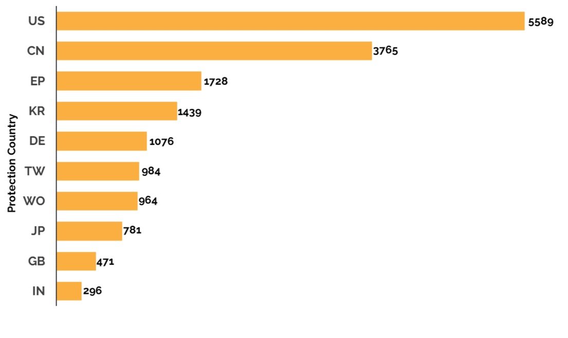
Geographical distribution and count of Patent Families (Source: Lumenci)
Conclusion
To conclude, HBM is a breakthrough memory solution for performance, power, and form factor constrained systems, delivering high-bandwidth, low effective power, and small form factor. Unlike conventional memory setups where DRAM chips are placed as close as possible on a circuit board, HBM stacks a bunch of RAM dies on top of each other.
*Disclaimer: This report is based on information that is publicly available and is considered to be reliable. However, Lumenci cannot be held responsible for the accuracy or reliability of this data.
*Disclaimer: This report is based on information that is publicly available and is considered to be reliable. However, Lumenci cannot be held responsible for the accuracy or reliability of this data.
Sourabh Thapar
Senior Associate at Lumenci
Sourabh is an Senior Associate at Lumenci. He holds a master’s degree in VLSI Design from IIT Dhanbad. He is interested in Portfolio Analysis and Damage estimation and is inclined toward Semiconductor and Wireless Communication. He likes to read about new technologies. He enjoys watching cricket and listing to music for leisure.