
Device Delayering for Reverse Engineering of Semiconductor Chips

Digital consumer products such as mobile phones, laptops, air conditioners, televisions, cameras, washing machines, etc., have become a necessity in our daily life. Semiconductors play a significant role in the operation of these devices. For example, chips used in laptops and mobile phones and temperature sensors used in air conditioners are semiconductors. Other than consumer products, advanced medical care, automobiles, bank ATMs also use semiconductor chips and make our life easier.
But what is a semiconductor? Semiconductors are underlying materials of electronic circuits whose conductivity lies between an insulator with almost no conductivity and a conductor with almost complete conductivity. In other terms, a semiconductor is a material that partly conducts current. Many semiconductors are crystals made of certain materials, such as silicon or germanium.
Due to their compact, reliable, and low-cost nature, these devices are used in various applications. They can be used as discrete components, like power devices, optical sensors, and light emitters, including solid-state lasers. They can also be integrated into complex but readily manufacturable microelectronic circuits. Thus, they are used by the manufacturing companies as a part of complex, advanced, and high-in-demand devices. But for a manufacturing company to be the latest in the market, it is crucial to be aware of what the competition is doing as part of business requirements. In this way, Reverse Engineering (RE) of competitors' products is an excellent strategy for gaining a competitive advantage. RE helps to understand what is inside a product or manufactured from scratch. RE can be done in various ways, e.g., product teardown, system-level analysis, process analysis, or circuit extraction on a wide range of devices, right from a semiconductor chip to an aircraft. The semiconductor industry's product teardown is not enough because advanced technologies integrate billions of components into a single product. A simple product teardown cannot give insights into the product's composition. Thus, complex RE techniques are applied to semiconductor devices. Due to this, RE has become a specialized job in the semiconductor industry.
This blog focuses on the device delayering process, which is a crucial step in both Processes and Material Analysis and Circuit Extraction performed on semiconductor chips. Circuit Extraction is becoming increasingly complex with each new generation of IC chips. Also, semiconductor devices are becoming increasingly compact day by day. Due to this, the designs may include an increasing number of layers, three-dimensional (3D) vertical stacking, air gaps, and different material compositions (e.g., Silicon Nitride, Silicon dioxide, Aluminum, Copper, Tungsten, Titanium, Titanium Nitride, and other low-k dielectrics). These devices may also have many logic gates and massive analog, RF, memory, and other macro-cell areas. Other devices such as MEMs, inductors, etc., can also be integrated on the chip depending upon the end-use. Therefore, device delayering has become inevitable to analyze the integrated circuits of a high-density semiconductor device. For this, the individual layers of the semiconductor device are removed in a controlled manner from top-down.
A single device sample at each metal layer and the polysilicon transistor gate level are created for device delayering of logic circuits. Each layer is accurately stripped off, one at a time, while keeping the surface planar. This requires comprehensive steps for the removal of each layer. These steps include methods such as plasma (dry) etching, wet etching, and polishing depending upon the material property of the discrete layers of the chip. Some of these techniques and methods are described below:
Wet Chemical Etch: In this process, a liquid solution is spread over the die surface to react with the surface materials. This produces liquid and gas, which diffuse away from the surface. Wet etching can be done using sulfuric or nitric acid, as they have high etched rates and works well when the die size is smaller than a package. Wet etching is a selective process depending on the liquid solution's chemical. In the case of selective etching, further steps are required to remove the residual materials. After wet etching, the die is usually rinsed with deionized water, acetone, and isopropyl alcohol.
Mechanical Polishing: This process is performed by mechanically rubbing the surface using tools and abrasives. The surface is smoothened to achieve the desired macroscopic and microscopic texture.
Dry Plasma Etch: This technique is performed to remove organic and other semiconductor materials using plasma. It is a readily controllable method through RF power, pressure, time, and gas selection. This process consumes minimum raw materials compared to the wet chemical etch or mechanical polishing. Unlike acid etchants, a plasma etchant is an excellent cleaning agent and can remove unwanted organic residues from metal surfaces. Further, plasma etching can stick two surfaces much better when compared to other etchants.

Parallel plate plasma etching configuration (Ref: Lumenci)
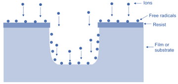
Interaction of the plasma with the substrate and mask
4. Reactive Ion Etching: Reactive Ion etching (RIE) is an ion-assisted reactive plasma etching process. The substrate or thin films are etched in a low-pressure chamber by the radio frequency (RF) discharge-excited species (radicals, ions, etc.). The excellent controllability of the etching behaviour allows RIE to produce topographical structures for micro and nanosystems.
While investigating an unknown chip, it is customary to start with a cross-sectional analysis of the chip to analyze the material composition and/or process technology nodes. The analysis of cross-sections can be performed using scanning electron microscopes (SEM), transmission electron microscopes (TEM), and other techniques to discover the composition and thickness of the desired layers. With today's generation of chips, device delayering combines over a hundred such methods, depending on various processes and materials used for building the chips. Some of these techniques are briefly described below:
Scanning electron microscopy (SEM): SEM is a technique where an electron beam is created and passed through a series of lenses and apertures. This electron beam is fired through an electron gun, and it produces a focused beam that strikes on the sample's surface to create magnified images of an object.
Transmission Electron Microscopy (TEM): TEM is a technique in which a high electron beam is passed on a thin specimen, and then the interaction between the electrons and atoms are used to observe the various features of the specimen such as crystal structure, features in dislocations and grain boundaries, and microscopic nature of defects. The drawback of TEM is that samples must be mechanically and chemically thinned first to ~0.15 micron to allow the electron beam to traverse the sample.
Focused Ion Beam (FIB): Focus Ion Beam (FIB) techniques are the most popular technique for delayering semiconductor devices. FIB method performs very precise nano machining and produces minute components or removes unwanted material. It is done using the sputtering process by careful control of the energy and intensity of the ion beam. As a result, FIB provides higher removal rates but is limited in the effective area revealed per unit time.
Scanning Tunnelling Microscopy (STM): A very sharp conductive tip is brought within tunneling distance (sub-nanometer) of a conductive sample surface and measures the tunneling current between the conductive tip and the sample surface when a potential is applied between them. There is a strong dependence of tunneling current on the tip-sample distance (i.e., the width of the vacuum gap or insulator air gap), so the convoluted information it provides is composed of (a) topographical changes and (b) surface electronic anisotropy.
EDX: In EDX spectroscopy, an element is identified by measuring the number and energy of X-rays emitted from a specimen after excitation with an electron beam. It is also known as energy dispersive spectroscopy and can be abbreviated as EDS, EDX, EDXS, or XEDS. The working of EDX is based on electron focusing, the same as in SEM. EDX is typically inbuilt within the SEM setup. The main advantage of EDS is that a broad range of elements can be examined synchronously.
Device Delayering in IP Litigation Cases
Lumenci has summarized below how device delayering was crucial in finding relevant evidence to support the infringement claims in a couple of complaints in recent IP litigation cases filed in the US.
In an IP Litigation Case (6:20-cv-00178 IP Edge v. Micron) filed in the US, both SEM and TEM analyses were performed on Micron's memory chips after device delayering specific layers of the chips to gather evidence as proof of infringement. As discussed above, one or more of the commonly used techniques for device delayering were used for performing process and material analysis to show that the accused semiconductor memory device (DRAM chip) included a capacitor insulating film. In addition, evidence was also gathered to show that the length of a portion where the opposing capacitors are overlapped in the mask layout is set so that the value of the parasitic capacitance between adjacent cell capacitors is not more than 10% of the set cell capacitance value.
In another complaint filed in an IP Litigation case (6:21-cv-00183 Nitride v. Lite-On), reverse engineering (particularly, TEM) of the accused product was performed after device delayering for gathering evidence to prove infringement. Here, the plaintiff alleged that the defendant infringed a patent based on products containing AlGaN-based UV LEDs manufactured and sold by the defendant. Specifically, the patent claims explained the structure of a light-emitting element comprising a gallium nitride-based semiconductor. TEM analysis showed that the second gallium nitride-based semiconductor layer is an AlGaN layer with a varied compositional ratio due to having higher Ga concentrations based on the contrast in the TEM images.
The above two cases show the importance of device delayering as a valuable reverse engineering tool to gather evidence for patent litigation cases involving semiconductor chips as accused products. The choice of device delayering and material characterization techniques for a specific combination of accused product and claim terms in the patents at issue determine the likelihood of winning the IP Litigation case. Accordingly, developing a strategy for reverse engineering a semiconductor chip at an early stage of litigation is crucial for our client's success. Learn more about Lumenci's semiconductor reverse engineering services here.
*Disclaimer: This report is based on information that is publicly available and is considered to be reliable. However, Lumenci cannot be held responsible for the accuracy or reliability of this data.
*Disclaimer: This report is based on information that is publicly available and is considered to be reliable. However, Lumenci cannot be held responsible for the accuracy or reliability of this data.
Author

Nupur Pandey
Senior Associate Consultant at Lumenci
Nupur is a VLSI Design Expert at Lumenci. She has experience in Semiconductor Technology, Patent Infringement Analysis, OTT, and Cloud Networking. Nupur holds a master's degree in VLSI Design from IIT Dhanbad.