
Through-Silicon-Via (TSV) Technology
Future electronic device development is anticipated to be significantly impacted by the Through-silicon-via technology, a type of VIA (Vertical Interconnect Access) connection used in IC packaging that makes vertical electrical connections between silicon wafers or dies.

Introduction
During the early days of the semiconductor industry, various circuit modules, like microprocessors, memory, mixed-signal devices, etc., were located on separate dies on a printed circuit board. System-on-chip (SoC) technology provides high circuit density by integrating many circuits on a single die, but the benefits of SoC are limited to the types of circuits involved. Many devices like sensors, memory, microprocessors, and MEMS devices are not easily integrated into a single due to different fabrication process flow. Different advanced packaging methods are required to integrate these devices. Initially, SIP (System-in-package) used 2D packaging technology to integrate different semiconductor dies into a single package. Still, these 2D ICs are limited by constraints of large layout space, high power consumption, high manufacturing cost, and technology scaling, creating a barrier to devise integration. Due to the increasing demand for small and compact electronic devices, semiconductor industries are leading towards developing three-dimensional (3D) SIP technology to develop 3D ICs. The core technology behind these 3D ICs is TSVs.
Through-Silicon Via (TSV) Technology, Advantages, and Applications
Through-Silicon Via (TSV) is a technology that has emerged in the fabrication of three-dimensional integrated circuits (3D ICs) as a solution to overcome the limitation of traditional two-dimensional integrated circuits (2D ICs). A Through-Silicon via (TSV) is a type of VIA (Vertical Interconnect Access) connection used in IC packaging technology that creates vertical electrical connections between silicon wafers or dies. These vertical connections can be used to interconnect multiple chips, memory, sensors, and other modules to create smaller, faster, and more power-efficient devices.
This technology is used as an alternative to wire-bond and flip chips (basically used in 2D IC Packaging Technology) to create 2.5D and 3D packages and 3D integrated circuits. One of the primary advantages of TSV technology is its ability to enhance the data transfer rates of the chips. With traditional interconnects in the 2D ICs, data signals travel laterally through the silicon substrate, resulting in a longer signal propagation delay. Using TSVs, data signals can travel vertically throughout the thinner silicon substrate, reducing signal propagation delay over several orders of magnitude. With TSVs, the reduced interconnect length with short vertical connections through the thinner silicon die makes them helpful in reducing the overall area and power consumption of the chip. These benefits make it him ideal for use in different high-speed applications such as data centers, servers, graphic processing units (GPUs), artificial intelligence (AI) based processors, and several wireless communication devices.
Another significant advantage of TSV technology is its ability to enable heterogeneous integration. Heterogeneous integration involves combining multiple chips from different technologies and manufacturers into a single package, allowing them to give better functionality and performance. TSVs enable these features by providing a reliable interconnect technology for the respective chips.

TSV technology offers several benefits to a wide variety of applications
Different types of IC Packaging
2-Dimensional Integrated Circuits (2D IC):
This is the traditional method of packaging ICs which involves mounting the IC chip onto a flat surface like a PCB (Printed Circuit Board) and connecting to a substrate using wire bonds or solder bumps. This substrate provides mechanical support for the IC chips and acts as a platform for connecting these IC chips to other components in the system. 2D IC packaging is mostly used where the size and cost of the package are not critical factors.
2.5-Dimensional Integrated Circuits (2.5D IC):
2.5D IC packaging involves stacking multiple IC chips near each other and connecting them using Through-Silicon Vias (TSVs) through an interposer. The interposer provides a high-density interconnect between the IC chips and also serves as a thermal management solution. The interposer may also contain passive components such as capacitors, inductors, and resistors, which can further reduce the overall size and cost of the package.
3-Dimensional Integrated Circuits (3D IC):
3D IC packaging is an advanced type of packaging that involves stacking multiple IC chips tier-to-tier on top of each other and connecting them using Through-Silicon Vias (TSVs). This type of packaging provides the highest level of integration density and offers the best performance with the smallest form factor.
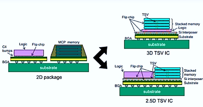
Different IC Packaging Technology
Fig.1: Image showing different IC packaging technology
Different Types of TSV Technology
Several types of TSV technologies have opted to address different design and performance requirements. Some of the kinds of TSV technology are:
Via First:
In this type of technology, TSVs must be connected to the integrated circuits' active layers (including transistors, resistors, capacitors, etc.). TSVs are created before the operational circuitry is fabricated (FEOL, i.e., Front end of the line) on the silicon wafer. This Via First approach is commonly used in the applications such as Image sensors, MEMS devices, etc.
Via Middle:
In this type of technology, TSVs are created after the active circuitry is fabricated on the wafer but before the fabrication of metallization layers (BEOL, i.e., the Back end of the line). This Via Middle approach is primarily used to connect both the active and passive layers of the integrated circuits through TSVs. This approach is mainly used in the applications such as Microprocessors, Memory devices, etc.
Via Last:
In this type of Technology, TSVs are fabricated after the fabrication of active layers, i.e., FEOL, and after (or during) the metallization layers, i.e., BEOL. This, Via the Last approach, connects the TSVs to the external package or substrate. This approach is often used in microelectronic systems.
The choice of TSV technology depends upon the specific design requirements and performance goals of the Integrated circuits (ICs). However, manufacturers use single and multiple types of TSV technology in their integrated circuits (ICs).
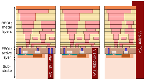
Types of TSV Technology
Fig.2: Image showing different types of Through-Silicon-Via (TSV) Technology (Source)
Fabrication of TSV
TSV fabrication involves several steps using specialized equipment and processes in a cleanroom environment. Some basic steps start with the cleaning (removing impurities) of the silicon wafer surface, followed by photoresist patterning (defining the location and shape of TSV). The wafer then goes through dry or wet etching to create the desired trench for TSV formation in the wafer. Further, the oxide and seed barrier layer formation can be done to prevent the diffusion of impurities in the wafer and provides electrical insulation. The trench is then filled with a conductive material such as copper, tungsten, titanium, etc. At last, planarization can be done on the surface of the wafer.


Figure 3: TSV Fabrication Process (Source: Lumenci)
Market Players in TSV IC Packaging
The growing demand for miniaturized semiconductor chips and their applications in different sectors such as telecommunications, automotive, healthcare and industrial manufacturing, aerospace and defense, and consumer electronic devices, including smartphones, laptops, desktops, notebooks, and tablets, etc., is accelerating the growth of Through-Silicon Via (TSV) Technology technology market globally.
Some of the market players who are involved globally in the Through-Silicon Via (TSV) IC Packaging industry are:
Xilinx
Texas Instruments
HuaTian Technology
IBM
Amkor technology
ALLVIA Inc.
Intel
Samsung Electronics
IP Moats in Through-Silicon Via (TSV) Technology
As the massive demand for high-performance compact devices in the electronics market, several companies and their collaborated research and development unit utilized their time and money and actively filed patents in this domain. TSMC Ltd. is a dominant player in this domain whose patents are related to the TSV fabrication methods, TSV designs for stacking 3D IC, TSV structures related to the packaging, etc. Intel and Qualcomm hold near the same positions whose patents are related to the TSV for transistor density scaling, packaging for stacked ICs, TSV testing processes in 3D ICs to make them defect-free, TSV interconnections, etc.

Top Optimized Assignees
Other key players who have filed patents in this technology are Global Foundries, IBM, Samsung Electronics, Xilinx, Texas Instruments, etc.

Technology Domain
As per our analysis, these patents are related to different technology domains, among which the semiconductor technology is on the top, that benefit from the TSV technology.
For example, Samsung Electronics is using TSV technology in 3D chip-Packaging for stacking 12 DRAM chips. Samsung DDR5 512GB RAM Module uses TSV Technology to stack eight layers of 16 GB DRAM chips to reach 512 GB capacity, uses 8 layers of CMOS Image sensors to adopt the TSV technology to form high-density interconnects widely used in smartphones, laptops, tablets, cars, industrial and medical equipment, security systems, and other consumer products having cameras. For example, Sony uses TSV technology to interconnect CMOS Image sensors with DRAM and smartphone image signal processors.
STMicroelectronics patented technology called ThELMA (Thick Epitaxial Layer for Micro-gyroscopes and Accelerometers) is manufacturing many MEMS devices such as accelerometers, gyroscopes, and smart sensors responsible for sensing acceleration, rotation, angular rate, vibration, displacement, heading, and other physical and environmental properties. STM is using its patented TSV technology in high-volume MEMS production.
AMS OSRAM is known for its high-volume manufacturing of extremely precise, miniaturized optics, sensors, and modules using TSV technology for IC packaging.

Country-wise Assignees
Graph shows that the companies that have built strong IPMoats in the last decade (2013-2022) are the United States, followed by China, Korea, Japan, Germany, Taiwan, Europe, the UK, France, and India.
*EP filings represent filings directly in the EPO office, and DE & GB represent filing in their respective offices.
Outlook
TSV Technology has revolutionized the semiconductor industry by enabling the development of more advanced and compact devices. TSVs play an essential role in developing semiconductor chips by providing benefits such as reduced interconnect length, high data transfer rates, improved power performance, high bandwidth memory, better signal integrity, reduction in the size of ICs, smaller form factor, etc. Active researchers and manufacturers are continuously working on designing and implementing TSV technology in semiconductor chips. Overall, TSV technology represents a significant role in the history of IC packaging, and it is expected to impact the development of future electronic devices profoundly.
Disclaimer: This report is based on information that is publicly available and is considered to be reliable. However, Lumenci cannot be held responsible for the accuracy or reliability of this data.
Disclaimer: This report is based on information that is publicly available and is considered to be reliable. However, Lumenci cannot be held responsible for the accuracy or reliability of this data.
Author
Mayank Gupta
Senior Associate Consultant at Lumenci
Mayank is a Senior Associate at Lumenci with 7+ years of experience in semiconductor device and photomask fabrication. He has co-authored several research papers in the semiconductor domain. His work at Lumenci includes delivering multiple services like Patent Infringement Analysis, Technical Analysis, and EoU/Claim Charts in Semiconductors, Telecommunication, Networking, and Digital Payments domains.