TFT Backplanes: Shaping the Generations of Display Technologies

Introduction
TFT Backplanes play an important role in the field of Display technologies. Basically, a Display Panel consists of two segments namely Frontplane and Backplane. The Frontplane (also called as screen) is primarily a group of pixels which collectively works and gives you an Image, and the Backplane, which has a matrix of TFT’s that controls the pixels. This type of LCD and OLED Display Panels is used in various smartphones, tablets, laptops, notebooks, wearables devices, automotive displays, and several other electronic consumer products.
Let’s first talk about what is TFT and a Pixel. A Thin film transistor (TFT) is basically made up of layers of thin films and act as a switch to control the flow of electric current required to turn ON/OFF the pixel. Thin film transistor (TFT) is also responsible to alter the brightness and colours of a pixel by regulating the flow of current.
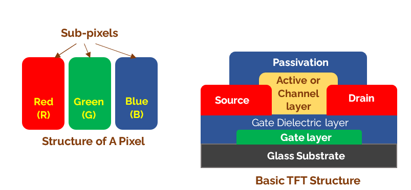
A Pixel consists of three different sub-pixels having colours, Red (R), Green (G), and Blue(B) combinedly called (RGB) which gives different colours to the images on the Frontplane. A Thin Film Transistor (TFT) is associated with each pixel and operated while applying a particular voltage.
So, the question that can come in our mind is how thin film transistor is made and how this operates a particular pixel. Each TFT consists of several layers like gate layer, gate dielectric layer, active layer or channel layer, source/drain layers, passivation layers etc. Several deposition techniques like Sputtering, Atomic Layer Deposition (ALD), Chemical Vapour Deposition (CVD) etc. are used to deposit all these layers under constrained environment to fabricate a thin film transistor on a glass substrate.
Basic TFT Structure
When a particular voltage is applied to the gate terminal, current flows between the source/drain terminal through an active layer or channel layer.
This current (flow of electrons) further drives the pixel and allows it to show different colors and brightness on the Frontplane (screen). A combination of pixels gives you an image like what you see on smartphones, televisions, wearables, etc. When such TFTs are arranged in the form of a matrix on a glass substrate, it is collectively called a TFT Backplane.
Types of TFT Backplanes
TFT Backplanes can be categorized by the different materials used to deposit the active layer or channel layer. Currently, commercial backplanes are based on the following TFT technologies:
Amorphous Silicon (a-Si)
Low-Temperature Polysilicon (LTPS)
Oxide Semiconductor (oxide)
Amorphous silicon (a-Si) is one of the elemental materials used to deposit active layer and composed of an amorphous solid having an irregular arrangement of atoms. The fabrication process of these types of TFT backplanes are easy, having low manufacturing costs and high yield as compared to other TFT technologies. This makes them possible to manufacture big sized display panels. In the beginning, a-Si TFT’s backplanes were used to fabricate LCD display panels, however, due to an irregular arrangement of atoms, their electron mobility is very slow which can also affect the signal propagation rate. This can also relate as a determining factor in terms of refresh rate, display resolution, and power consumption.

a-Si & LTPS
Low-Temperature Polycrystalline Silicon (LTPS) and Oxide semiconductor (Oxide) Technology came into the display market to overcome these issues.
LTPS fabrication process is the recrystallization of a-Si molecules to Polycrystalline Silicon with the help of an Excimer laser annealing process. The process occurs at relatively low temperatures when compared with High-Temperature Polycrystalline Silicon, which is why it is called Low-Temperature Polysilicon. This results in higher electron mobility i.e., more than 100 times faster than amorphous silicon (a-Si) which gives faster switching display panels. One of the advantages with LTPS Technology is that it offers high aperture ratio in LCD Display panels, which helps reduce backlight power consumption.
Also, due to the fabrication of small TFT size in LTPS Backplanes, power consumption is also very less. The prominent feature in the LTPS technology is that accessibility of CMOS (Complementary Metal oxide semiconductor) technology that includes both n-channel type and p-channel type thin film transistors for fabrication of Backplanes which is not available in a-Si technology (only n-MOS structure) and Oxide technology (only n-MOS structure). Also, LTPS Backplane offers high ON current which gives faster switching and less parasitic capacitance (due to small size transistors) which combinedly makes it more suitable for high resolution and better refresh rate display panels. But the large complexities in the manufacturing processes, and high materials costs makes it more challenging towards fabricating big sized display panels. Therefore, LTPS backplanes are mostly used in small and medium sized high-end LCD and OLED display panels for smartphones, and wearable devices.
On the other hand, Oxides TFT’s backplanes uses Amorphous Indium Gallium Zinc Oxide (a-IGZO), and other types of Amorphous Oxide semiconductor materials as active layer or channel layer. Oxide TFT backplanes (a-IGZO) having better electron mobility (around 20 to 50 times more as compared with a-Si TFT backplanes), small transistor sizes (as compared with amorphous silicon backplanes) enable low power consumption and low manufacturing costs (as compared with LTPS backplanes) and make them promising candidate over huge display panels market. Also, a-IGZO TFT backplanes offers wide band gap, hence small OFF current as compared with a-Si TFT backplanes or LTPS backplanes results less power dissipation.
Oxide TFT backplanes can be highly scalable to big-sized high resolution display panels with less manufacturing cost as compared with LTPS backplanes. Several research are ongoing in oxide TFT technologies and LTPS TFT technology to improve the display panels in terms of refresh rate, manufacturing costs, power dissipation etc.
LTPO (Low-Temperature Polycrystalline Oxide), which is now-a-days, a new emerging technology and is basically a combination of both LTPS TFT’s and Oxide TFT’s Technology. In this, some TFT’s are fabricated using LTPS technology and some TFT’s are fabricated using Oxide (a-IGZO) technology. LTPO backplanes having variable refresh rates and improved power consumption efficiency make them useful in high-end flagship devices. Apple introduced this technology first in September 2014, as LTPO backplane in the Apple Watch series 4. Samsung, also having a similar type of technology (so called HOP technology, short form of hybrid oxide and polycrystalline silicon) introduced LTPO backplane in the Galaxy Note series smartphones. LG display also has a similar type of technology.
Several research are ongoing in the TFT domain w.r.t. its top gate structures, self-aligned structures, fabrication processes with using different materials to make better TFT backplanes on a glass substrate (mother glass), flexible substrates, etc. Now, the next thing that can come in our mind is the glass substrate and Mother glass as used for the displays. Let’s discuss about these two terms.
Display glass substrate and Mother glass
Display glass substrate plays an important role in manufacturing TFT backplanes. These glass substrates are a specific type of glass which are thermally stable, strong, durabile and can support most of the TFT technologies while achieving the required resolution. As the current market requirements moves continuously from mid-size to large-size display panels for televisions and other electronic devices, this creates new challenges and opportunities for display glass substrate manufacturers to increase the yields, maximize throughput with low manufacturing costs.
The basic properties which the glass substrates should fulfil are that it must have minimum total thickness variations (TTV), low sag, and low total pitch variations (TPV). During TFT Backplane manufacturing process, display glass substrate will go through several fabrication processes and between these processes, glass substrate will deform in term of shape or size (also called as strain) that arises the term variation in total pitch (TPV). Less variation in total pitch gives better display glass substrate. Also, during the TFT backplane manufacturing process, display glass substrate will go through several depositions and naturally bend due to their weight, which defines the term Sag. Low sag property of big sized display glass substrate gives better stability and durability with low manufacturing costs. When we talk about big sized display glass substrates, the variation in thickness of glass defines the term total thickness variation (TTV). Minimum total thickness variations give uniform layer thickness with better control during TFT backplane fabrication processes.
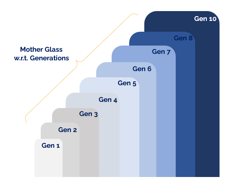
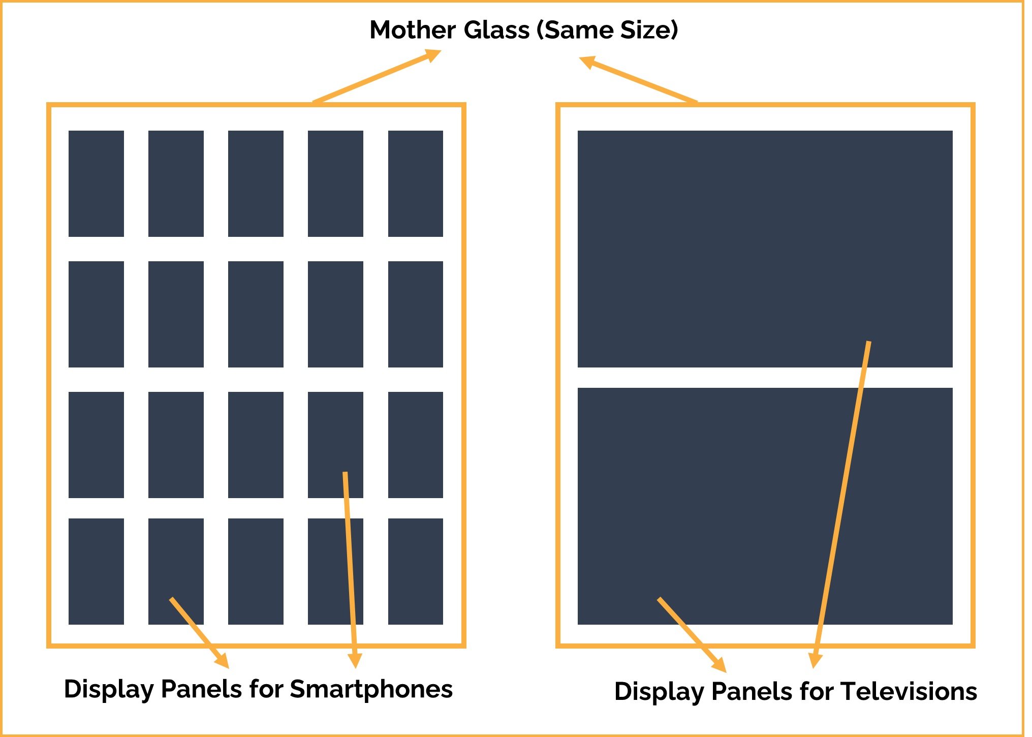
Now, at this point of time, we all know that display glass substrate will act as a base for making TFT backplanes. Mother glass is a term which indicates a very large size of glass substrate which goes through different fabrication processes, and at last, cut into several sizes which is individually used in as Display glass substrates in smartphones, televisions, wearables, automobile industry etc. Size of the “Mother glass” is determined by the term “Generation”. Newer generation represents bigger size of mother glass when compared with older generations. For example, Gen 10 glass has a very large size of mother glass compared to Gen 1 glass.
Mother Glass and Panels
Sizes of the mother glass in different generation will slightly differ in case of different manufacturers. Multi model glass is a term that refers to cutting different size of display glass substrates from the mother glass with a good cutting efficiency to minimize the manufacturing costs Several research activities are ongoing to improve the quality of Mother glass with reasonable manufacturing costs.
Major Players and Patenting Activities
Some of the Key Players across the globe who are supplier in the field of glass substrate are:
Corning Incorporated
AGC Incorporated
LG Chem
SCHOTT Ag
Tungshu Optoelectronics
IRICO Group New Energy Company Limited
CGC Glass (Central Glass Co. Ltd.)
AvanStrate Incorporated
Nippon Electric Glass
Some of the Key Players across the globe who are in the field of TFT Backplanes are:
BOE Technology Group Co. Ltd.
AUO Corporation
Japan
Display Inc
LG Display
Panasonic
Visionox
Foxconn
Samsung Display
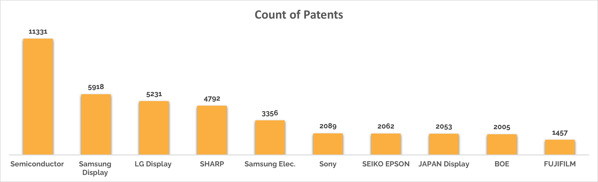
Patent Publication Trends for Companies (Source: Lumenci)
In addition to the above data, there are several other joint venture companies, research institution collaborators, and academic institutions that are actively participating in the research and development field of TFT backplanes and display glass. Some of the key players across the globe who falls under this domain and act as assignees in terms of Patent filing can be seen in the respective graph.
The below graph (left) shows the trend of filing the number of patents by the key players over the last 20 years. It seems that actively research and development work is ongoing in the field of TFT backplanes and display glass. The below graph (right) shows the involvement of different countries/regions in terms of Patent filing over the last 20 years by the key players. It shows that different countries/region across the globe are actively involved in the development of TFT backplanes and display glass.

Patent Publication Trends (Source: Lumenci)

Patent Publication Trends across the Globe (Source: Lumenci)
Conclusions
The Display market, nowadays, is abundantly using the LTPS TFT Backplane Technology for high-end small and mid-size LCD, OLED display panels in smartphones, wearables devices and Oxide TFT Backplane Technology for small to big-sized LCD, OLED display panels in laptops, televisions, smartphones, wearable devices, automotive displays, and other electronic consumer devices. Compatibility of these technologies also enables the Display panel manufacturers to use it as 3D displays, transparent or flexible displays.
The revenues generated from various market segments in the field of Oxide-TFT and LTPS-TFT Backplanes are nowadays in millions of dollars, and it is expected to reach in billions of dollars in the upcoming years.
At last, it is not wrong in saying that the necessity of the TFT backplanes is increasing day-by-day in shaping the future of Display industries. With the current limited natural resources across the globe, researchers are working 24x7 to improve the overall efficiency of Oxide TFT and LTPS TFT backplanes in terms of high-resolution, higher driving currents, low power consumption, variable refresh rate, and with low manufacturing costs.
Author

Mayank Gupta
Senior Associate Consultant at Lumenci
Mayank is a Senior Associate at Lumenci with 7+ years of experience in the semiconductor device and photomask fabrication. He has co-authored several research papers in the semiconductor domain. His work at Lumenci in multiple services like Patent Infringement Analysis, Technical Analysis, and EoU/Claim Charts in Semiconductors, Telecommunication, Networking, and Digital Payments domains. He holds a Bachelor of Engineering (B.E.) degree in Electronics and Instrumentation from MITM Indore and Master of Technology (MTech.) degree in Microelectronics and VLSI Design from Motilal Nehru National Institute of Technology (MNNIT), Allahabad, India.